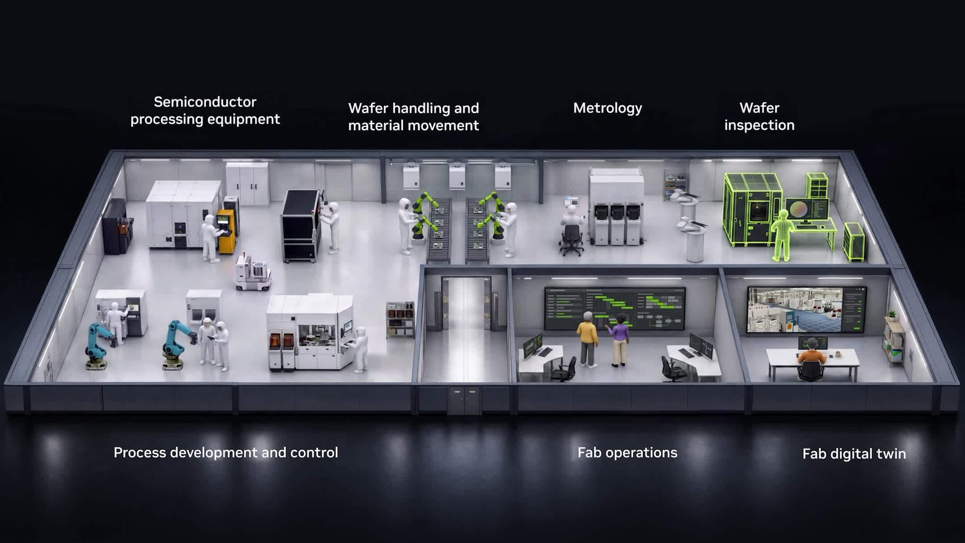
manufacturers face rising demand for advanced chips alongside growing process complexity and tighter error margins. NVIDIA outlines how AI is reshaping fab operations by accelerating simulation, replacing time-consuming physical trials with learned physics models, and deploying to handle design, testing and manufacturing decisions faster.
The approach, called an AI-defined fab, lets engineers get answers to critical questions—how process changes will behave, how materials will interact with new steps, and where defects originate—much more quickly than traditional methods. This reduces iteration cycles and improves yield.
This is an AI-written summary. The original reporting belongs to NVIDIA Blog. How we write these · Spot a mistake?